Published On Jul 19, 2023
You can buy it on Amazon: https://amzn.to/3rxnlQ4
If you wanna buy the tester of POWER-Z, you can visit our Amazon store:
https://www.amazon.com/s?me=A31UM8SRX...
Introduction
---------------------------------------------------------------
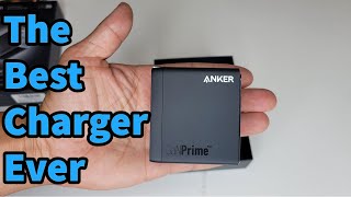
Today, we gonna take apart this 150W GaN charger from the Anker GaNPrime series. It's equipped with three USB-C and a USB-A ports.
This means you can fast charge up to four devices simultaneously.
We can also call it "747 Charger". Let's go ahead and see how can it be so small but powerful.
Bill of materials (BOM)
------------------------------------------
Model: A2340
Time-delay Fuse: BetterFuse
Y Capacitor: DGCX
Safety X2 Capacitor: DGCX
Film Capacitor: DGCX
PFC Controller: ON Semiconductor NCP1623
GaN IC (PFC boost): Navitas NV6136A
PFC Boost Rectifier: ON Semiconductor MURF860
Electrolytic Capacitor: Yongming
Primary Controller: Infineon XPDS2201
Primary GaN IC: Infineon IGI60F1414A1L
Synchronous Rectification Controller: MPS MP6951
Synchronous Rectifier: Infineon BSC0802LS
Solid Capacitor: Yongming
Optocoupler: CT1018
SMD Y Capacitor: TRX TMY1102M
Protocol Chip: Ismartware SW3536
Buck MOSFET: Infineon BSZ018N04LS6, Infineon BSZ063N04LS6
Output VBUS MOSFET: Infineon BSZ018N04LS6
Current Sense Amplifier: SG-Micro SGM8199A1
MCU: Eastsoft ES8P5066FJNK
Chapter
----------------------------------
0:00 Intro
1:40 Test
2:37 Teardown
3:29 Analysis
8:04 Summary
For more details. You can visit our website: https://www.chargerlab.com
For Business Inquiries: [email protected]
SOCIALS:
Instagram: / chargerlabs
Facebook: / chargerlab
Twitter: / chargerlab
Telegram: https://t.me/ChargerLABchannel